- 您现在的位置:买卖IC网 > Sheet目录983 > HI5767EVAL2 (Intersil)EVALUATION PLATFORM HI5767
�� �
�
�Application� Note� 9762�
�converter� is� approximately� 1.5V.� Therefore,� the� duty� cycle� of�
�the� sampling� clock� should� be� measured� at� the� 1.5V� trigger�
�level� of� the� HI5767� sample� clock� input� pin.�
�The� sinewave� to� logic� level� comparator� drives� a� series� of�
�additional� inverters� that� provide� isolation� between� the� three�
�sample� clocks� used� on� the� evaluation� board.� One� clock� is�
�used� to� drive� the� converter� sample� clock� input� pin� and� the�
�other� two� provide� CLK� and� CLK� at� the� data� output�
�header/connector,� P2.� The� clock/data� relationship� at� the� P2�
�output� connector� is� as� follows.� CLK� has� rising� edges� aligned�
�with� digital� data� transitions� and� CLK� has� rising� edges�
�aligned� mid-bit.�
�The� data� corresponding� to� a� particular� analog� input� sample�
�will� be� available� at� the� digital� outputs� of� the� HI5767� after� the�
�data� latency� (7� cycles)� plus� the� HI5767� digital� data� output�
�delay.�
�The� sample� clock� and� digital� output� data� signals� are� made�
�available� through� two� connectors� contained� on� the� evaluation�
�board.� Line� drivers� are� not� provided� for� the� digital� output� data�
�and� it� should� be� pointed� out� that� the� load� presented� to� the�
�converter� digital� output� data� signals,� D0� -� D9,� should� not�
�exceed� the� data� sheet� CMOS� drive� limits� and� a� load�
�capacitance� of� 10pF.� The� P1� 96-pin� I/O� connector� allows� the�
�evaluation� board� to� be� interfaced� to� the� DSP� evaluation�
�locked� to� each� other� to� ensure� coherence.� The� output� of� the�
�signal� generator� driving� the� ADC� analog� input� is� bandpass�
�?ltered� to� improve� the� harmonic� distortion� of� the� analog� input�
�signal.� The� comparator� on� the� evaluation� board� will� convert�
�the� sine� wave� CLK� input� signal� to� a� square� wave� at� TTL� logic�
�levels� to� drive� the� sample� clock� input� of� the� HI5767.� The�
�ADC� data� is� captured� by� a� logic� analyzer� and� then�
�transferred� over� the� GPIB� bus� to� the� PC.� The� PC� has� the�
�required� software� to� perform� the� Fast� Fourier� Transform�
�(FFT)� and� do� the� data� analysis.�
�Coherent� testing� is� recommended� in� order� to� avoid� the�
�inaccuracies� of� windowing.� The� sampling� frequency� and�
�analog� input� frequency� have� the� following� relationship:� f� I� /f� S� =�
�M/N,� where� f� I� is� the� frequency� of� the� input� analog� sinusoid,�
�f� S� is� the� sampling� frequency,� N� is� the� number� of� samples,�
�and� M� is� the� number� of� cycles� over� which� the� samples� are�
�taken.� By� making� M� an� integer� and� odd� number� (1,� 3,� 5,� ...)�
�the� samples� are� assured� of� being� nonrepetitive.�
�Refer� to� the� HI5767� data� sheet� for� a� complete� list� of� test�
�de?nitions� and� the� results� that� can� be� expected� using� the�
�evaluation� board� with� the� test� setup� shown.� Evaluating� the�
�part� with� a� reconstruction� DAC� is� only� suggested� when�
�doing� bandwidth� or� video� testing.�
�boards� available� from� Intersil.� The� digital� output� data� and�
�sample� clock� can� also� be� accessed� by� clipping� the� test� leads�
�HP8662A�
�REF�
�HP8662A�
�of� a� logic� analyzer� or� data� acquisition� system� onto� the�
�header/connector� pins� of� connector� P2.�
�The� A/D� converters� OE� control� input� pin� allows� the� digital�
�output� data� bus� of� the� converter� to� be� switched� to� a� three-�
�BANDPASS�
�FILTER�
�state� high� impedance� mode.� This� feature� enables� the� testing�
�CLK�
�V� IN�
�EVALUATION� BOARD�
�and� debugging� of� systems� which� are� utilizing� one� or� more�
�converters.� This� three-state� control� signal� is� not� intended� for�
�use� as� an� enable/disable� function� on� a� common� data� bus�
�and� could� result� in� possible� bus� contention� issues.� The� A/D�
�converters� OE� control� input� pin� is� controlled� by� the�
�installation� or� removal� of� a� shunt,� JP1,� contained� on� the�
�evaluation� board.� Installation� of� JP1� forces� the� OE� control�
�input� pin� low� for� normal� operation� while� removal� of� JP1�
�allows� the� digital� output� data� bus� of� the� converter� to� be�
�switched� to� a� three-state� high� impedance� mode.�
�HI5767� Performance� Characterization�
�Dynamic� testing� is� used� to� evaluate� the� performance� of� the�
�HI5767� A/D� converter.� Among� the� tests� performed� are�
�Signal-to-Noise� and� Distortion� Ratio� (SINAD),� Signal-to-�
�Noise� Ratio� (SNR),� Total� Harmonic� Distortion� (THD),�
�Spurious� Free� Dynamic� Range� (SFDR)� and� Intermodulation�
�Distortion� (IMD).�
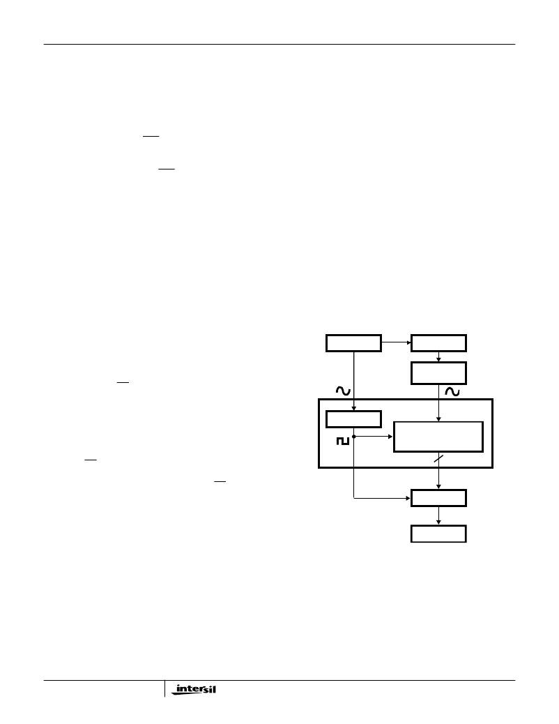
�Figure� 4� shows� the� test� system� used� to� perform� dynamic�
�testing� on� high-speed� ADCs� at� Intersil.� The� clock� (CLK)� and�
�analog� input� (V� IN� )� signals� are� sourced� from� low� phase� noise�
�HP8662A� synthesized� signal� generators� that� are� phase�
�3-4�
�COMPARATOR�
�V� IN�
�CLK� HI5767�
�DIGITAL� DATA� OUTPUT�
�HI5767EVAL2�
�14�
�DAS9200�
�GPIB�
�PC�
�FIGURE� 3.� HIGH-SPEED� A/D� PERFORMANCE� TEST� SYSTEM�
�发布紧急采购,3分钟左右您将得到回复。
相关PDF资料
HI5805EVAL1
EVALUATION PLATFORM HI5805
HI5828EVAL2
EVALUATION PLATFORM HI5828
HI5960SOICEVAL1
EVALUATION PLATFORM SOIC HI5960
HI7188EVAL
EVALUATION PLATFORM HI7188
HI7190EVAL
EVALUATION PLATFORM HI7190
HJ4-L-DC12V
RELAY GEN PURPOSE 4PDT 5A 12V
HL2-HP-AC100V-F
RELAY GEN PURPOSE DPDT 10A 100V
HLM01510Z16K50JJ
RES 16.5K OHM 15W 5% WW
相关代理商/技术参数
HI5780
制造商:INTERSIL 制造商全称:Intersil Corporation 功能描述:10-Bit, 80 MSPS, High Speed, Low Power D/A Converter
HI5780-EV
制造商:INTERSIL 制造商全称:Intersil Corporation 功能描述:10-Bit, 80 MSPS, High Speed, Low Power D/A Converter
HI5780JCQ
制造商:Rochester Electronics LLC 功能描述:32 PQFP COMTEMP VIDEO D/A 10BIT 80MHZ - Bulk 制造商:Harris Corporation 功能描述:
HI5780JCQ-T
制造商:Rochester Electronics LLC 功能描述:HI5780JCQ IN TAPE & REEL - Bulk
HI5800
制造商:INTERSIL 制造商全称:Intersil Corporation 功能描述:12-Bit, 3MSPS, Sampling A/D Converter
HI5800_00
制造商:INTERSIL 制造商全称:Intersil Corporation 功能描述:12-Bit, 3MSPS, Sampling A/D Converter
HI5800BID
制造商:INTERSIL 制造商全称:Intersil Corporation 功能描述:12-Bit, 3MSPS, Sampling A/D Converter
HI5800-EV
制造商:Rochester Electronics LLC 功能描述:- Bulk